


Metrology for Laser Optics
This is Sections 15.1, 15.2, 15.3, 15.4, 15.5, and 15.6 of the Laser Optics Resource Guide.
Metrology is crucial for ensuring optical components consistently meet their desired specifications and function safely. This reliability is especially important for systems utilizing high-power lasers or where changes in throughput may cause inadequate system performance. A wide range of metrology is used to measure laser optics including cavity ring down spectroscopy, atomic force microscopy, differential interference contrast microscopy, interferometry, Shack Hartmann wavefront sensors, and spectrophotometers.
Cavity Ring Down Spectroscopy
Cavity ring down spectroscopy (CRDS) is a technique used to determine the composition of gas samples, but for laser optics it is used to make high sensitivity loss measurements of optical coatings. In a CRDS system, a laser pulse is sent into a resonant cavity bounded by two highly-reflective mirrors. With each reflection, a small amount of light is lost to absorption, scattering, and transmission while the reflected light continues to oscillate in the resonant cavity. A detector behind the second mirror measures the decrease in intensity of the reflected light (or “ring down”), which is used to calculate the loss of the mirrors (Figure 1). Characterizing the loss of a laser mirror is essential for ensuring a laser system will achieve its desired throughput.
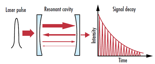
Figure 1: Cavity ring down spectrometers measure the intensity decay rate in the resonant cavity, allowing for higher accuracy measurements than techniques that just measure absolute intensity values
The intensity of the laser pulse inside the cavity (I) is described by:
I0 is the initial intensity of the laser pulse, Ƭ is the total cavity mirror loss from transmission, absorption, and scattering, t is time, c is the speed of light, and L is the length of the cavity.
The value determined in CRDS is the loss of the entire cavity. Therefore, multiple tests are required in order to determine the loss of one mirror. Two reference mirrors are used to make an initial measurement (A), and then two more measurements are taken: one with the first reference mirror replaced by the mirror being tested (B) and one with the other reference mirror replaced by the test mirror (C). These three measurements are used to determine the loss of the test mirror.
M1 and M2 are the loss of the two reference mirrors and M3 is the loss of the test mirror. The loss from air in the cavity is assumed to be negligible. CRDS is an ideal technique for characterizing the performance of reflective laser optics because it is much easier to accurately measure a small amount of loss rather than a large reflectance (Table 1). Transmissive components with anti-reflection coatings can also be tested by inserting them into a resonant cavity and measuring the corresponding increase in loss. CRDS must be performed in a clean environment with meticulous care, as any contamination on the mirrors or to the inside of the cavity will affect the loss measurements.
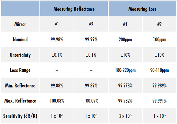
Table 1: The sensitivity of measuring the reflectance of a mirror directly with an uncertainty of ±0.1% is two orders of magnitude greater than measuring the mirrors loss with an uncertainty of ±10%. This demonstrates that loss measurements for highly reflective mirrors are much more accurate than reflectance measurements
To learn more about CRDS and its benefits for measuring high reflectivity laser mirrors, watch the webinar recording below.
Interferometry
Interferometers utilize interference to measure small displacements, surface irregularities, and changes in refractive index. They can measure surface irregularities <λ/20 and are used to qualify flats, spherical lenses, aspheric lenses, and other optical components.
Interference occurs when multiple waves of light are superimposed and added together to form a new pattern. In order for interference to occur, the multiple waves of light must be coherent in phase and have non-orthogonal polarization states.1 If the troughs, or low points, of the waves align they cause constructive interference add their intensities, while if the troughs of one wave align with the peaks of the other they will cause destructive interference and cancel each other out (Figure 2).
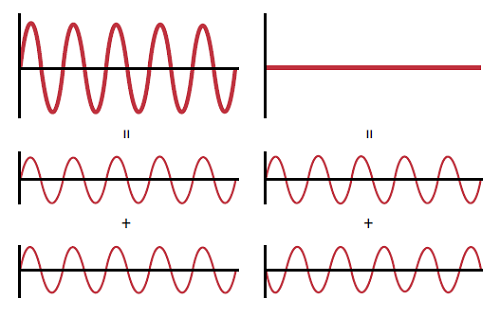
Figure 2: Interferometers us constructive interference (left) and destructive interference (right) to determine surface figure, as differences in surface figure between the test optic and reference optic cause a phase difference that results in visible interference fringes
Interferometers typically use a beamsplitter to split light from a single source into a test beam and a reference beam. The beams are recombined before reaching a photodetector, and any optical path difference between the two paths will create interference. This allows for comparing an optical component in the path of the test beam to a reference in the reference beam (Figure 3). Constructive and destructive interference between the two paths will create a pattern of visible interference fringes. Both reflective and transmissive optical components can be measured by comparing the transmitted or reflected wavefront to a reference.
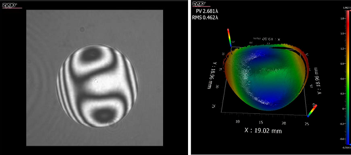
Figure 3: Sample image from an interferometer showing bright areas where the test and reference beams constructively interfered and dark rings where they destructively interfered (left), as well as the resulting 3D reconstruction of the test optic (right)
There are several common interferometer configurations (Figure 4). Mach–Zehnder interferometers utilize one beamsplitter to separate an input beam into two separate paths. A second beamsplitter recombines the two paths into two outputs, which are sent to photodetectors. Michelson interferometers use a single beamsplitter for splitting and recombining the beams. One variant of Michelson interferometers are Twyman–Green interferometers, which measure optical components with a monochromatic point source as the light source. Fizeau interferometers utilize a single beamsplitter oriented perpendicularly to the beamsplitter in Michelson interferometers, which causes the system to only require one mirror. Fabry–Pérot interferometers allow for multiple trips of light by using two parallel partially transparent mirrors instead of two separated beam paths.
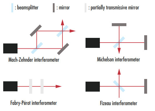
Figure 4: Various common interferometer configurations
Dust particles or imperfections on optical components that make up an interferometer, besides the optic being tested, can lead to optical path differences that may be misconstrued as surface defects on the optic. Interferometry requires precise control of the beam paths, and measurements may also be subject to laser noise and quantum noise.
Short Coherence Length Interferometry
Some unique interferometer configurations, such as short coherence length and photothermal common-path interferometers, serve a different purpose than conventional interferometers. Short coherence length interferometers use specialized LEDs as their illumination source instead of a laser.2 The LED has a coherence length longer than a typical LED but less than that of a laser. This allows the system to measure parallel, flat surfaces while minimizing reflections from back surfaces (Figure 5).
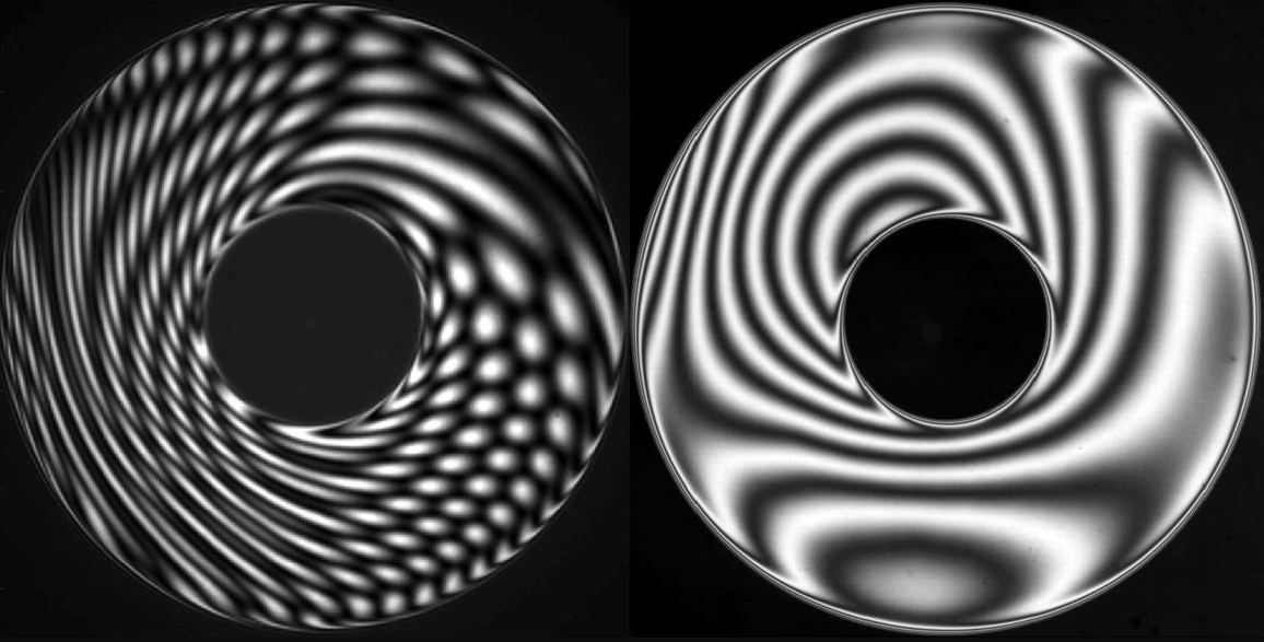
Figure 5: Short coherence length interferometers using specialized LEDs as their light source are able to measure parallel, flat surfaces without noise from light reflecting off of the back surface (right), while conventional laser-based interferometers will be affected by this noise (left). Image from InterOptics LLC2
In order to measure parallel flat surfaces on windows, laser crystals, and other optics using a conventional interferometer, Vaseline or another substance must be applied to the back surface to prevent light from reflecting off of it and interfering with measurements of the front surface. Applying this additional substance reduces noise but increases the time it takes to record measurements, as it must be applied, cleaned off, then reapplied to measure the other surface, then cleaned before coating. The most effective way to clean away Vaseline is vinegar, and this poses the risk of staining certain materials that are sensitive to acids. This technique is also not effective for optics having a much lower or higher refractive index than glass and is completely ineffective if the back surface has been coated.
Using a specialized LED with a short coherence length allows the front surface of an optic to be isolated from the rear surface, eliminating the need for special treatment of the rear surface. This minimizes measurement time, the risk of damage to the part, and the risk of inaccurate measurements.2 However, because the coherence length is short there is a limited range of where the surface being measured must be placed in order to resolve interference fringes. One benefit of this limited measurement range is that it prevents dust, scratches, and other defects in the optical train outside of the limited measurement window from affecting measurements (Figure 6). This technique is also less sensitive to vibration by design and does not need to be placed on an expensive vibration isolation table.
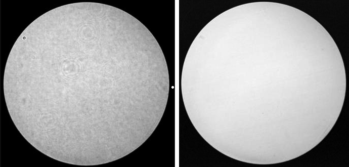
Figure 6: Dust, scratches, and other defects in the optical train of conventional interferometers will show up as artifacts during measurement (left) but these defects will not impact measurements taken using a short coherence length interferometer (right). Image from InterOptics LLC2
Photothermal Common-Path Interferometry
Photothermal common-path interferometers (PCIs) use a focused pump beam to heat a target area while a single probe beam experiences phase distortion because of thermal expansion and the resulting change in refractive index.3 PCIs provide accurate measurements of absorption, allowing for better characterization of the spectral properties of optical coatings.
The phase of the probe beam is distorted in the heated area while the pump beam is active. This distortion generates a second weak wave with its phase shifted by half of a period relative to the stronger, undistorted probe beam wave.3 Interference between these two waves does not occur right away, but at some distance further from the sample (Figure 7). The heating will apply a similar phase shift to the reflection of the probe beam from the front surface, allowing for either transmission or reflection measurement of the surface absorption.
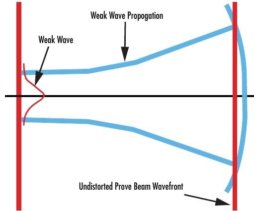
Figure 7: Thermal distortion creates a weak, second wave from the probe beam in a photothermal common-path interferometer, and this secondary wave generates an interference pattern with the undistorted probe beam later in the system3
An optical chopper is typically used to break up a continuous wave (CW) laser source and periodically heat the sample. After transmitting through the sample, the probe beam passes through an aperture before its periodic distortion is measured (Figure 8). The final signal is proportional to absorption in the sample, allowing for accurate absorption measurement.
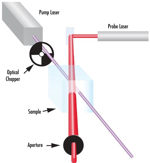
Figure 8: Typical schematic of a photothermal common-path interferometer3
These absorption measurements provide valuable information for better understanding the spectral properties of optical coatings and bulk substrates. For example, two different anti-reflection coatings could have similar measured reflectivity values, but the true performance of the coatings is not understood without also understanding the effects of absorption and scatter, as two coatings could have identical reflectivities but different absorption values.
PCIs measure absorption more accurately than spectrophotometers, which determine absorption by directly measuring transmission.3 Spectrometers can struggle to measure low absorption levels. PCIs can also separate measurements of absorption in the coating from absorption in the bulk substrate.
Atomic Force Microscopy
Atomic force microscopy (AFM) is a technique that provides surface topography with atomic resolution (Figure 9). An extremely small and sharp tip scans across a sample’s surface, resulting in a 3D reconstruction of the surface. The tip is attached to a rectangular or triangular cantilever that connects to the rest of the microscope head. The cantilever’s motion is controlled by piezoelectric ceramics, which ensures 3D positioning of the cantilever with subnanometer resolution.4
In laser optics, AFM is primary used to calculate an optical component’s surface roughness, which may significantly affect the performance of a laser optical system as it is often the main source of scattering. AFM can provide a 3D map of a surface with a precision of a few Angstrom’s.5
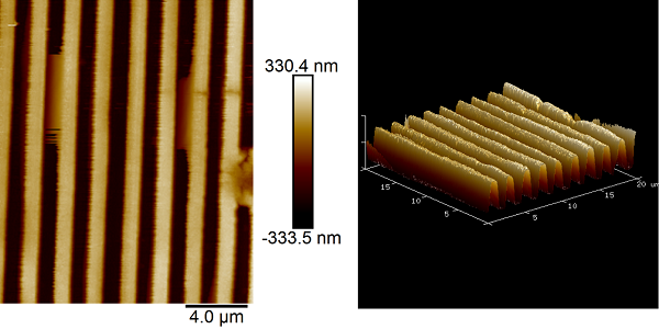
Figure 9: Atomic force microscopy produces nanometer-level topography maps, which can be useful for characterizing gratings
The tip is either scanned across the sample while in constant contact with the system, known as contact mode, or in intermittent contact with the surface, known as tapping mode. In tapping mode, the cantilever oscillates at its resonant frequency, with the tip only contacting the surface for a short time during the oscillating cycle. Contact mode is less complicated than tapping mode and provides a more accurate reconstruction of the surface. However, the possibility of damaging the surface during scanning is higher and the tip wears out faster, leading to a shorter lifetime of the tip. In both modes, a laser is reflected off the top of the cantilever onto a detector. Changes in the height of the sample surface deflect the cantilever and change the position of the laser on the detector, generating an accurate height map of the surface (Figure 10).

Figure 10: Changes in surface topography move the AFM tip, changing the position of the reflected laser on the detected and allowing for surface topography measurement
The shape and composition of the tip play a key role in the spatial resolution of AFM and should be chosen according to the specimen requiring a scan. The smaller and sharper the tip, the higher the lateral resolution. However, small tips have longer scanning times and a higher cost than larger tips.
Control of the distance between the tip and the surface determines the vertical resolution of an AFM system. Mechanical and electrical noise limit the vertical resolution as surface features smaller than the noise level cannot be resolved.6 The relative position between the tip and the sample is also sensitive to the expansion or contraction of AFM components as a result of thermal variations.
AFM is a time-consuming metrology technique and is mainly used for process validation and monitoring, where a small fraction of a sample surface on the order of 100μm x 100μm is measured to provide a statistically significant representation of its manufacturing process as a whole.
White Light Interferometry for Superpolished Surface Roughness Measurement
White light interferometry (WLI) can also be used to measure surface roughness. The combination of AFM and WLI allows optical fabricators to measure surface topography over a wide range of spatial frequencies, even measuring the sub-angstrom RMS surface roughness of superpolished surfaces.
Most interferometers utilize a monochromatic laser as the illumination source because the laser’s long coherence length makes it easy to observe interference fringes, but white light interferometers utilize a broadband illumination source to analyze surface height. Surface height can be measured because the interference at a given location is highest when the reference and measured optical path lengths are equal, so modulating the distance between the WLI and the test surface generates surface topography data. White light interferometers are typically Michelson interferometer setups with the test optic placed in one arm and a reference optic in the other (Figure 11). The length of the reference arm is varied by translating the reference optic through some range.
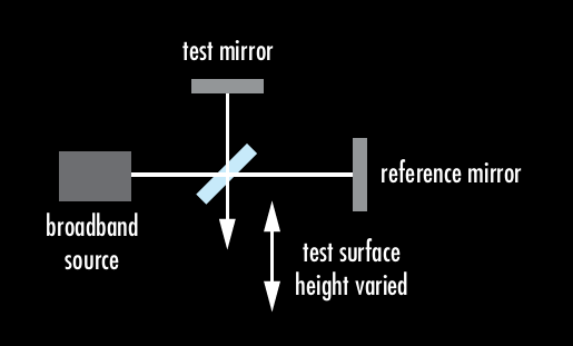
Figure 11: Schematic of a typical white light Michelson interferometer used to determine surface roughness. The instrument is kept stationary as the height of the test surface is varied.
WLI and AFM have overlapping spatial frequency ranges and can both be utilized for measuring sub-angstrom surface roughness of superpolished surfaces (Table 2), which instrument is better is dependent on the spatial frequency range being measured.7 It is widely accepted that optics intended to be used in the visible spectra do not need to be measured beyond ~2000 cycles/mm, which is ideal for WLI. However, for optics intended to be used in the UV spectra the higher spatial frequency range of the AFM may be required. The AFM can also measure lower spatial frequencies (as seen in Table 2), but other factors make AFM less production friendly. Due to longer measurement times, AFM has an extreme sensitivity to temperature fluctuations and external vibrations. Therefore, AFM is better suited for the controlled environment of a test lab while WLI is better suited for a factory setting.
| Instrument | Lower Spatial Frequency Limit [cycle/mm] | Upper Spatial Frequency Limit [cycle/mm] | Note |
| White Light Interferometer (Zygo NewView) |
1 3 5 9 25 40 |
50 90 180 360 900 1,800 |
(Objective mag.) 2.75 5 10 20 50 100 |
| Atomic Force Microscope | 30 35 45 60 90 185 |
8,000 9,600 12,000 16,000 24,000 50,000 |
Depending on tip radius and instrument setup |
Table 2: Reasonable spatial frequency ranges of a white light interferometer with interchangeable objectives and an atomic force microscope7
Shack-Hartmann Wavefront Sensors
A Shack-Hartmann wavefront sensor (SHWFS) measures the transmitted and reflected wavefront error of an optical component or system with high dynamic range and accuracy. The SHWFS has become very popular due to its ease of use, fast response, relatively low cost, and ability to work with incoherent light sources.
The wavefront of an optical wave is a surface over which the wave has a constant phase. Wavefronts are perpendicular to the direction of propagation, therefore collimated light has a planar wavefront and converging or diverging light has a curved wavefront (Figure 12). Aberrations in optical components lead to wavefront errors, or distortions in transmitted or reflected wavefronts. By analyzing transmitted and reflected wavefront error, the aberrations and performance of an optical component can be determined.
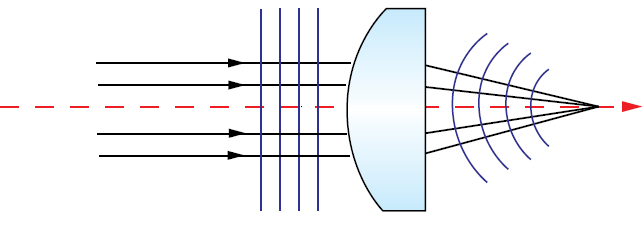
Figure 12: Perfectly collimated light has a planar wavefront. Light diverging or converging after a perfect, aberration-free lens will have a spherical wavefront
SHWFS utilizes an array of microlenses, or lenslets, with the same focal length to focus portions of incident light onto a detector. The detector is divided in small sectors, with one sector for each microlens. A perfect planar incident wavefront results in a grid of focused spots with the same separation as the center-to-center spacing of the microlens array. If a distorted wavefront with some amount of wavefront error is incident on a SHWFS, the position of the spots on the detector will change (Figure 13). The deviation, deformation, or loss in intensity of the focal spots determines the local tilt of the wavefront at each of the microlenses. The discrete tilts can be used to recreate the full wavefront.
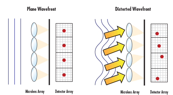
Figure 13: Any wavefront error present in light entering a SHWFS will lead to a displacement of the focused spot positions on the detector array
One advantage of SHWFS compared to interferometry is that the dynamic range is essentially independent of wavelength, offering more flexibility. However, the dynamic range of SHWFS is limited by the detector sector allocated to each microlens. The focal spot of each microlens should cover at least 10 pixels on its respective sector to achieve an accurate reconstruction of the wavefront. The larger the detector area covered by the focal spot, the greater the SHWFS’ sensitivity, though this comes with a tradeoff of shorter dynamic range. In general, the focal spot of the microlens should not cover more than half of the designated detector sector; this guarantees a reasonable compromise between sensitivity and dynamic range.8
Increasing the number of microlenses in an array results in an increase in spatial resolution and less averaging of the wavefront slope over the microlens aperture, but there are less pixels allocated to each microlens. Larger microlenses produce a more sensitive and precise measurement for slowly varying wavefronts, but this may not sufficiently sample complex wavefronts and result in an artificial smoothing of the reconstructed wavefront.9
Spectrophotometers
Spectrophotometers measure the transmission and reflectivity of optical components and are essential for characterizing the performance of optical coatings (Figure 14). A typical spectrophotometer consists of a broadband light source, a monochrometer, and a detector (Figure 15). Light from the light source is sent into the monochrometer’s entrance slit where it splits into its component wavelengths using a dispersive element such as a diffraction grating or prism. The monochrometer’s exit slit blocks all wavelengths except for a narrow band that passes through the slit, and that narrow wavelength band illuminates the test optic. Changing the angle of the diffraction grating or prism changes the wavelengths that pass through the exit slit, allowing the test wavelength band to be finely tuned. Light reflected or transmitted through the test optic is then directed onto a detector, determining the optic’s reflectivity or transmission at a given wavelength.
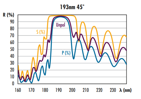
Figure 14: Sample reflectivity spectrum of a TECHSPEC® Excimer Laser Mirror captured using a spectrophotometer
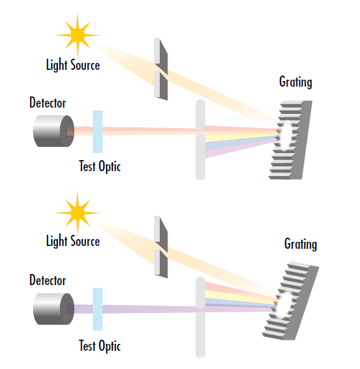
Figure 15: The test wavelength of a spectrophotometer can be finely tuned by adjusting the angle of the diffraction grating or prism in the monochrometer
The light source must be incredibly stable and have adequate intensity across a broad range of wavelengths to prevent false readings. Tungsten halogen lamps are one of the most commonly used light sources for spectrophotometers because of their long lifespan and ability to maintain a constant brightness.10 Multiple light sources covering different wavelength ranges are often used if a very broad total range is required.
The smaller the width of the monochrometer’s slits, the higher the spectral resolution of the spectrophotometer. However, reducing the width of the slits also reduces the transmitted power and may increase the reading acquisition time and amount of noise.12
A wide variety of detectors are used in spectrophotometers as different detectors are better suited for different wavelength ranges. Photomultiplier tubes (PMTs) and semiconductor photodiodes are common detectors used for ultraviolet, visible, and infrared detection.8 PMTs utilize a photoelectric surface to achieve unmatched sensitivity compared to other detector types. When light is incident on the photoelectric surface, photoelectrons are released and continue to release other secondary electrons, which causes a high gain. The high sensitivity of PMTs is beneficial for low intensity light sources or when high levels of precision are required. Semiconductor photodiodes such as avalanche photodiodes are less expensive alternatives to PMTs; however, they have more noise and a lower sensitivity than PMTs.
While most spectrophotometers are designed for use in the ultraviolet, visible, or infrared spectra, some spectrophotometers operate in more demanding spectral regions such as the extreme ultraviolet (EUV) spectrum, with wavelengths from 10-100nm. EUV spectrophotometers typically use diffraction gratings with extremely small grating spacings to effectively disperse the incident EUV radiation.
Group Delay Dispersion Measurement
White light interferometers are used to measure the group delay dispersion (GDD) of both reflective and transmissive optical components. GDD is critical to the performance of ultrafast laser optics, as the short pulse duration of ultrafast lasers leads to significant chromatic dispersion in optical media. More information on GDD and ultrafast optics can be found in our Ultrafast Dispersion application note.
Most interferometers utilize a monochromatic laser as the illumination source because the laser’s long coherence length makes it easy to observe interference fringes, but white light interferometers utilize a broadband illumination source to analyze dispersion. White light interferometers are typically Michelson interferometer setups with the test optic placed in one arm and a reference optic in the other (Figure 16). The length of the reference arm is varied by translating the reference optic through some range.
Interferograms reveal signals whenever the optical path lengths of the two arms become identical, and the exact position at which this occurs is wavelength dependent. This allows for the optical path length difference between different wavelengths to be precisely determined, revealing the test optic’s GDD (Figure 16).
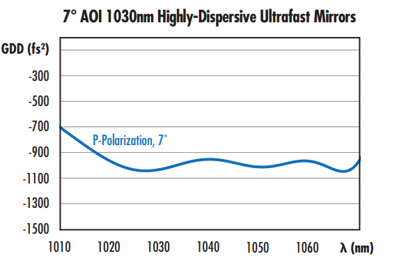
Figure 16: Plot of GDD vs. wavelength for a highly-dispersive ultrafast mirror obtained using white light interferometry
The signal is either detected by a photodetector or a spectrometer. Photodetectors integrate the signals of different wavelengths over time, and applying a Fourier transform algorithm to the captured interferograms reveals the wavelength-dependent GDD and chromatic dispersion.7 Using a spectrometer instead of a photodetector eliminates the need for a Fourier transfer of the captured data.
The sensitivity of photodetector-based white light interferometers is dependent on the step sizes of the stage used to translate the reference optic, but this is not an issue with spectrometer-based systems.
Differential Interference Contrast Microscopy
Differential interference contrast (DIC) microscopy is used for highly-sensitive defect detection in transmissive materials, particularly for identifying laser damage in optical coatings and surfaces (Figure 18). It is difficult to observe these features using traditional brightfield microscopy because the sample is transmissive, but DIC microscopy improves contrast by converting gradients in the optical path length from variations in refractive index, surface slope, or thickness into intensity differences at the image plane. Slopes, valleys and surface discontinuities are imaged with improved contrast to reveal the profile of the surface. DIC images give the appearance of a 3D relief corresponding to the variation of optical path length of the sample. However, this appearance of 3D relief should not be interpreted as the actual 3D topography of the sample.
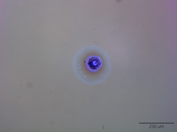
Figure 17: DIC microscopy converts gradients in optical path length into intensity differences at the image plane, allowing for visualization of laser-induced damage that would be otherwise hard to detect
DIC microscopy uses polarizers and a birefringent Wollaston or Nomarski prism to separate a light source into two orthogonally polarized rays (Figure 18). An objective lens focuses the two components onto the sample surface displaced by a distance equal to the resolution limit of the microscope. After being collimated by a condenser lens, the two components are then recombined using another Wollaston prism. The combined components then pass through a second polarizer known as an analyzer, which is oriented perpendicular to the first polarizer. The interference from the difference in the two component’s optical path length leads to visible brightness variations.
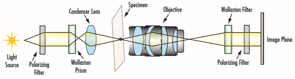
Figure 18: Typical DIC microscopy setup where a Wollaston prism splits the input beam into two separately polarized states
One limitation of DIC microscopy is increased cost compared to other microscopy techniques. The Wollaston prisms used to separate and recombine the different polarization states are more expensive than the components needed for microscopy techniques such as phase contrast or Hoffman modulation contrast microscopy.11
Video: Metrology at Edmund Optics®
WATCH NOW
Read About Our Metrology Program
LEARN MORE
References
- Hinterdorfer, Peter, and Yves F Dufrêne. “Detection and Localization of Single Molecular Recognition Events Using Atomic Force Microscopy.” Nature Methods, vol. 3, no. 5, 2006, pp. 347–355., doi:10.1038/nmeth871.
- InterOptics LLC. "Engineered coherence interferometry." InterOptics, 2018, http://www.inter-optics.com/tech.html
- Stanford Photo-Thermal Solutions. "Photothermal technology: common-path (single beam) interferometry." Stanford Photo-Thermal Solutions, Nov. 2021, https://www.stan-pts.com/howitworks.html
- Binnig, G., et al. “Atomic Resolution with Atomic Force Microscope.” Surface Science, vol. 189-190, 1987, pp. 1–6., doi:10.1016/s0039-6028(87)80407-7.
- Dr. Johannes H. Kindt. “AFM enhancing traditional Electron Microscopy Applications.” Atomic Force Microscopy Webinars, Bruker, Feb. 2013, www.bruker.com/service/education-training/webinars/afm.html.
- Murphey, Douglas B, et al. “DIC Microscope Configuration and Alignment.” Olympus, www.olympus-lifescience.com/en/microscope-resource/primer/techniques/dic/dicconfiguration/
- Paschotta, Rüdiger. Encyclopedia of Laser Physics and Technology, RP Photonics, October 2017, www.rp-photonics.com/encyclopedia.html.
- Forest, Craig R., Claude R. Canizares, Daniel R. Neal, Michael McGuirk, and Mark Lee Schattenburg. "Metrology of thin transparent optics using Shack-Hartmann wavefront sensing." Optical engineering 43, no. 3 (2004): 742-754.
- John E. Greivenkamp, Daniel G. Smith, Robert O. Gappinger, Gregory A. Williby, "Optical testing using Shack-Hartmann wavefront sensors," Proc. SPIE 4416, Optical Engineering for Sensing and Nanotechnology (ICOSN 2001), (8 May 2001); doi: 10.1117/12.427063
- Wassmer, William. “An Introduction to Optical Spectrometry (Spectrophotometry).” Azooptics.com, https://www.azooptics.com/Article.aspx?ArticleID=753.
More Resources
- Metrology at Edmund Optics: Measuring as a Key Component of Manufacturing Video
- Beam Expander Testing Application Note
- Laser Damage Threshold Testing Application Note
- Laser Damage Threshold Scaling Calculator
- Understanding Optical Specifications Application Note
- Laser Optics Lab Video Series


or view regional numbers
QUOTE TOOL
enter stock numbers to begin
Copyright 2024, Edmund Optics Singapore Pte. Ltd, 18 Woodlands Loop #04-00, Singapore 738100
California Consumer Privacy Acts (CCPA): Do Not Sell or Share My Personal Information
California Transparency in Supply Chains Act
This content may include material that has been generated or modified using artificial intelligence (AI).
The FUTURE Depends On Optics®